


QuantumDiamonds plans €152 million investment in quantum chip inspection facility in Munich

QuantumDiamonds (QD), a Munich-based quantum sensing company for semiconductor inspection, has unveiled plans to invest €152 million to build what it calls the world’s first production facility for advanced chip testing systems.
The planned Munich facility is “expected to receive tens of millions of euros in public support from the German federal and Bavarian governments under the European Chips Act.”
“The new site in eastern Munich sends a strong signal for the future of our microelectronics ecosystem. With its cutting-edge analysis technologies, QD shows how vital innovation is for Europe’s semiconductor competitiveness. The planned support from the federal and Bavarian governments is an investment in high-quality jobs, technological sovereignty, and our region’s progress,” stated Hubert Aiwanger, Bavarian Minister for Economic Affairs.
The new facility will include sensor production lines for quantum-grade diamond substrates, cleanroom integration of QDM inspection systems, joint development labs with semiconductor partners, as well as application support for fab integration and inline process control. Its construction is set to begin immediately.
QuantumDiamonds was founded in 2022 by Kevin Berghoff and Dr Fleming Bruckmaier to commercialise diamond-based quantum sensing. It was spun out from the Technical University of Munich. The company develops and deploys quantum sensing technologies and tools for the failure analysis and metrology of a new generation of semiconductor chips. It aims to disrupt conventional semiconductor testing methods and accelerate fault localisation deep within 3D semiconductor architectures.
QD has created diamond-based quantum sensors at the atomic scale, capable of operating in extreme conditions. “Non-destructive fault isolation in advanced packaging is an incredibly difficult challenge that the industry is still working on to solve. This technology shows significant promise in addressing that gap. By detecting magnetic fields to trace current, it offers a potential pathway to visualise defects that are currently invisible to standard thermal or X-ray tools,” explained Dr David Su, the previous director of TSMC’s failure analysis team and now a QD advisor.
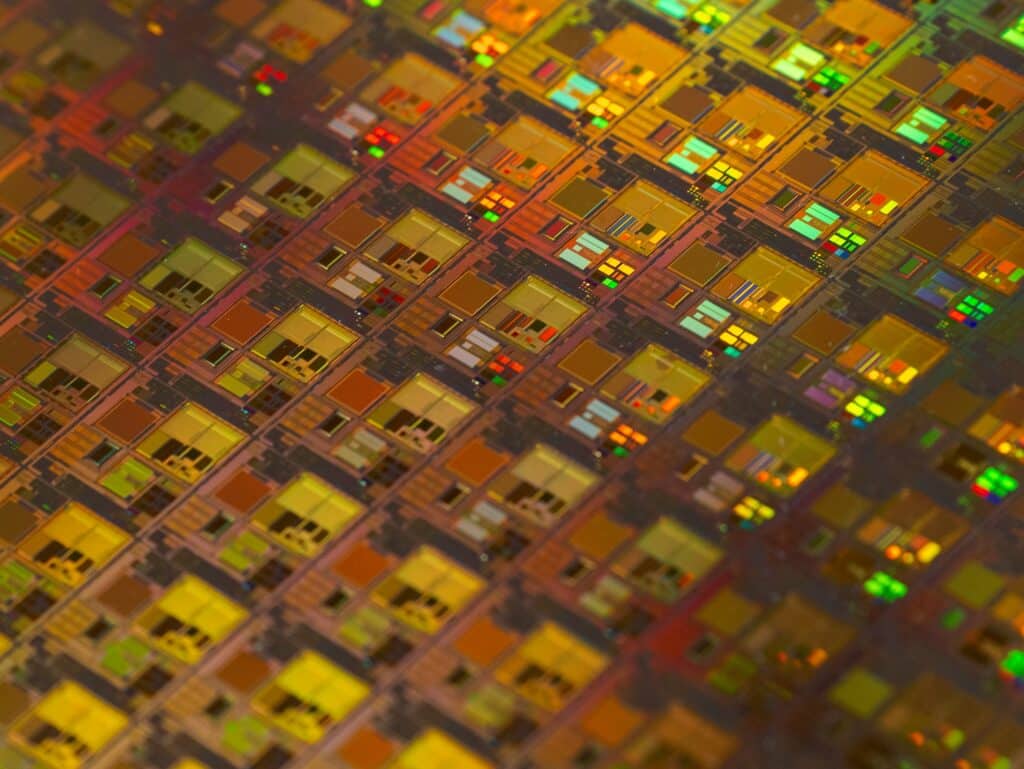
By harnessing nitrogen-vacancy (NV) centres in diamond, QD’s systems non-destructively map electrical current with micrometre-level precision in a matter of seconds, even within highly complex chip packages. This capability is especially critical for advanced 2.5D and 3D architectures that underpin AI, mobile, and automotive electronics, the company mentioned in the statement.
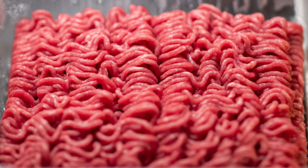
The company recently published a non-destructive failure analysis on Apple A12 chips fabricated by TSMC. QD used Quantum Diamond Microscopy (QDM) to localise buried defects within commercial package-on-package devices. It claims that these defects remain undetectable with conventional tools such as lock-in thermography and CT X-ray imaging.
QD claims that it is experiencing surging demand for its systems, having already completed proof-of-concept work with nine of the world’s ten largest semiconductor manufacturers. Initial deployments were completed in Europe, with further installations scheduled for Q1 2026 in both the United States and Taiwan.
“This investment marks our transition from research to global production. We’re building the tools the chip industry needs to inspect what was previously invisible—and doing it in Germany, with European IP and talent,” said Berghoff, CEO and co-founder of QD.
“The early support we received from programmes like the EIC Accelerator and SPRIN-D laid the foundation for this scale-up. With the expected Chips Act funding, we will move from pilot deployments to volume production, helping secure Europe’s role in the future of the semiconductor industry,” he added.
The post QuantumDiamonds plans €152 million investment in quantum chip inspection facility in Munich appeared first on EU-Startups.