


Swedish semiconductor startup AlixLabs closes €15 million Series A to scale atomic-level etching technology
AlixLabs, a Lund-based semiconductor startup specialising in Atomic Layer Etching (ALE) technology, has announced the closing of its €15 million Series A in the first quarter of 2026, following a strategic investment from Stephen Industries, a Finnish investment company.
In November 2025, AlixLabs announced that Global Brain and key institutional investors had subscribed to its Series A to the tune of €14.1 million, with the difference to the €15 million total remaining open until the first quarter of 2026.
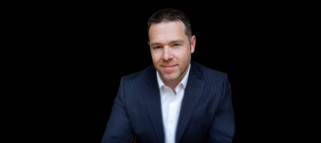
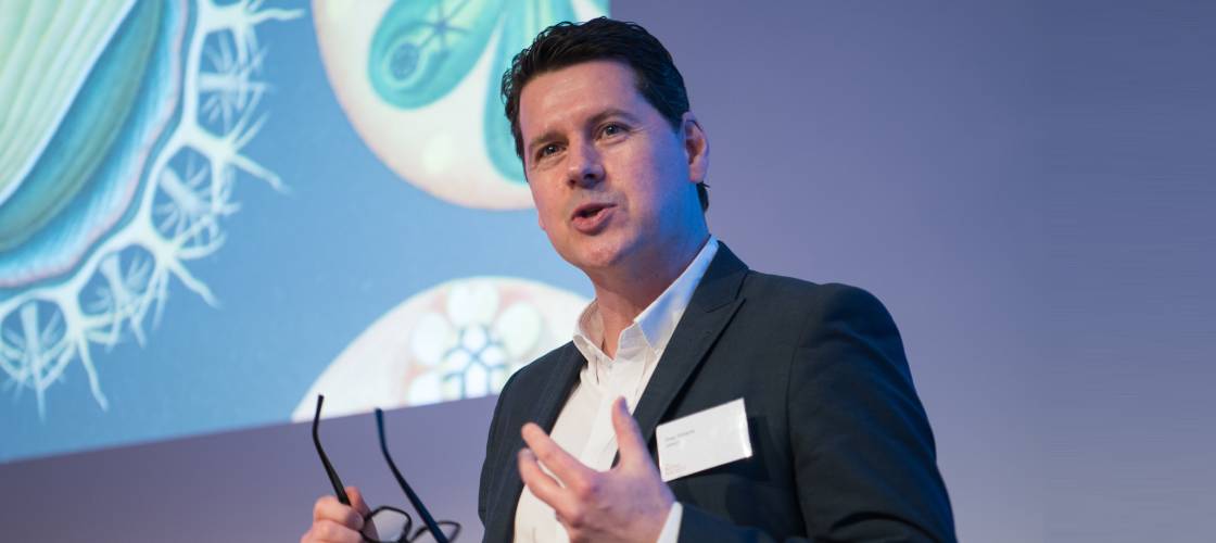
“Stephen Industries brings deep industrial expertise and a proven ability to scale companies in adjacent technology domains. Kustaa’s experience with Picosun is especially valuable as we move from development toward broader commercialisation of our APS platform,” said Jonas Sundqvist, CEO of AlixLabs.
Founded in 2019, AlixLabs claims to be the world’s only pure-play ALE company. Spun off from Lund University in Sweden, its mission is to make production of the semiconductors in the ångström (Å) era more accessible, sustainable and affordable.
It is a Swedish semiconductor industry supplier with equipment and processes capable of manufacturing nanostructures with characteristic sizes smaller than 20 nanometers. It enables energy-efficient fabrication of structures beyond the resolution limits of optical and electron beam lithography, through APS (Atomic Pitch Splitting).
According to the company, as chip complexity increases, so does the cost for both design and manufacture. AlixLabs claims to provide several ALE-based solutions for atomic-level processing that reduce the number of process steps required to manufacture a chip while increasing throughput.
The startup states that all its solutions integrate seamlessly into existing production workflows, making it more affordable to progress toward the ångstrom (Å) era. By utilising ALE, semiconductor companies can reduce consumption of power and water while reducing emissions.
“AlixLabs’ processes are designed for use on 300 millimetre (12-inch) logic and DRAM silicon wafers, including FinFET and GAAFET (nanowire). They are equally at home in 150 and 200-millimetre wafers for power electronics on gallium nitride (GaN),” explained the company.
AlixLabs states that this investment marks a strategic milestone for the company as it continues to develop its proprietary ALE solutions, particularly its flagship APS (Atomic Pitch Splitting) technology, which is aimed at enabling more precise, efficient, and cost-effective semiconductor fabrication.
A major aspect of the partnership is Kustaa Poutiainen from Stephen Industries, whose background in developing and expanding deep-tech firms offers substantial strategic benefit. Poutiainen was instrumental in the growth of Picosun, a Nordic Atomic Layer Deposition (ALD) company that rose to international prominence. Since ALD and ALE are closely related technologies, his experience is especially pertinent to AlixLabs’ objectives.
“AlixLabs operates in a highly promising space within semiconductor process technology. Having seen firsthand how ALD evolved from a niche innovation to a critical industry standard, I see strong parallels with ALE. AlixLabs has the potential to follow a similar trajectory,” said Kustaa Poutiainen, Chairperson and President of Stephen Industries.
The news funding will be used to accelerate product development, expand technical capabilities, and strengthen partnerships with semiconductor manufacturers.
The post Swedish semiconductor startup AlixLabs closes €15 million Series A to scale atomic-level etching technology appeared first on EU-Startups.